
An illustration of the difference between 2D or planar NAND flash and 3D Vertical NAND flash


Within a few years, you'll likely be carrying a smartphone, tablet or laptop with hundreds of gigabytes or even terabytes of hyper fast, non-volatile memory, thanks to two memory developments unveiled this week.
First, Samsung announced it is now mass producing three-dimensional (3D) Vertical NAND (V-NAND) chips; then start-up Crossbar said it has created a prototype of its resistive random access memory (RRAM) chip.
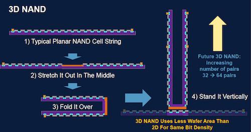
Three-dimensional NAND takes today's flash, which is built on a horizontal plane, and turns it sideways. Then, like microscopic memory skyscrapers, it stacks them side-by-side to create a vastly more dense chip with twice the write performance and 10 times the reliability of today's 2D, or planar, NAND.
The most-dense process for creating silicon flash memory cells to store data on planar NAND is between 10 nanometer (nm) and 19nm in size. To give some idea of how small that is, a nanometer is one-billionth of a meter -- a human hair is 3,000 times thicker than NAND flash made with 25nm process technology. There are 25 million nanometers in an inch.
NAND flash uses transistors or a charge to trap (also known as Charge Trap Flash) to store a bit of data in a silicon cell, while RRAM uses tiny conductive filaments that connect silicon layers to represent a bit of data - a digital one or a zero.
In RRAM, the top layer of silicon nitrate creates a conductive electrode, while the lower layer is non-conductive silicon oxide. A positive charge creates a filament connection between the two silicon layers, which represents a one; a negative charge breaks that filament, creating a resistive layer or a zero.
So, which memory tech wins?
Which of the two memories will dominate the non-volatile memory marketplace in five years isn't certain, as experts have mixed opinions about how much 3D (or stackable) NAND flash can extend the life of current NAND flash technology. Some say it will grow beyond Samsung's current 24 layers to more than 100 in the future; others believe it has only two to three generations to go, meaning the technology will hit a wall when it gets to 64 layers or so.
By contrast, RRAM starts out with an advantage. It is denser than NAND, with higher performance and endurance. That means RRAM will be able to use silicon wafers that are half the size used by current NAND flash fabricators. And, best of all, current flash fabrication plants won't need to change their equipment to make it, according to Crossbar CEO George Minassian.
"It will cost maybe a couple million dollars in engineering costs for plants to introduce it. That's what it is in our plan," Minassian said. "It's about the same cost as introducing a new [NAND flash] node, like going from 65 to 45 nanometer node."
Crossbar claims its RRAM technology has a 30 nanosecond latency time. Samsung's top-rated flash, the 840 Pro SSD, has a 0.057 millisecond latency. A millisecond is one-thousandth of a second, a nanosecond is one billionth of a second - a million times faster.
According to Minassian, RRAM can natively withstand 10,000 write-erase cycles, which is a little more than typical consumer-grade MLC (multi-cell level) NAND flash can withstand today - and that's without any error correction code. ECC is used to upgrade today's MLC NAND flash to enterprise-class flash cards and solid-state drives (SSDs).
In fact, Crossbar expects to see mass production of its RRAM chip in two years. Minassian said his company has already penned an agreement with a flash fabrication plant in the automotive industry to manufacture the chips. He also said an agreement with a much larger fab is nearing an agreement.
Both RRAM and 3D NAND herald an enormous leap in memory performance and storage capacity. Crossbar's RRAM promises 20 times faster write performance and 10 times the durability of today's planar NAND flash. Like 3D NAND, RRAM memory chips will be stacked, and a 1TB module will be roughly half the size of a NAND flash module with similar storage, Minassian said.
Three-dimensional NAND offers multiples more capacity. With every NAND flash "skyscraper" comes a doubling of capacity. Samsung said its V-NAND will initially only boast capacities ranging from 128GB to 1TB in embedded systems and SSDs, "depending on customer demand." So, Samsung appears to be betting on a manufacturing cost reduction - price per bit -- and not a capacity increase to drive V-NAND sales.
Crossbar's initial RRAM chip will also be capable of storing up to 1TB of data, but it can do that on a chip smaller than a postage stamp; that amounts to 250 hours of hi-def movies on a 200mm square surface.
When it comes to performance, RRAM brings yet another advantage. A NAND flash chip today has about 7MB/sec write speeds. SSDs and flash cards can achieve 400MB/sec speeds by running multiple chips in parallel.
A RRAM chip boasts 140MB/sec write speeds, and that's without parallel interconnects to multiple chips, Minassian said.
Both 3D NAND and RRAM's purported performance gains mean that storage devices will no longer be the system bottlenecks they are now. In the future, the bottleneck will be the bus -- the communication layer between computer components. In other words, if NAND flash is a 100 mph car and RRAM is a 200 mph car, it doesn't matter how fast they can go if the road they're on has a curve that limits speeds to 50 mph.
On top of performance, RRAM uses a fraction of the power to store data that NAND flash uses, meaning it will help extends battery life "to weeks, months or years," according to Crossbar.
For example, NAND flash requires about 20 volts of electricity to write a bit of data into a silicon chip. RRAM requires just 4 microamps to write a bit of data.
Crossbar is not alone in its development of RRAM. Both Hewlett-Packard and Panasonic have developed their own versions of resistive memory, but according to Jim Handy, principal analyst at Objective Analysis, Crossbar has a huge leg up on other developers.
"One very big advantage of this technology is that the selection device is built into the cell. In other RRAMs it is not, so something external (a diode or transistor) has to be built in. This is an area that has received a lot of research funding but is still a thorny issue for many other technologies," he said in an email reply to Computerworld
Handy said the market for alternative technologies to RRAM is limited, as flash manufacturers tend to use the cheapest technology they can get away with, even though other technologies offer better performance.
RRAM has the advantage
RRAM isn't the only memory advance in sight. Alternative forms of non-volatile memory that could be future rivals to NAND and DRAM include Everspin's magnetoresistive RAM (MRAM) and phase-change memory (PCM), a memory type being pursued by Samsung and Micron. There is also Racetrack Memory, Graphene Memory and Memristor, HP's own type of RRAM.
Gregory Wong, founder and principal analyst at research firm Forward Insights, believes Crossbar's RRAM is a viable product that may someday challenge NAND, "and when I say NAND, I mean 3D NAND, too," he said.
Racetrack memory still has at least five years go to go before it is even viable. "Right now, it looks like an interesting concept. Whether it eventually becomes commercialized or not is far out in the future," Wong said.
"Phase change..., well, there is some out there, but the question is, where does it fit in the memory market? Right now, it's a NOR replacement," Wong continued. "Its performance and endurance is like NOR, not NAND.
"Generally, when you look at...others touting RRAM, there's a lot of skepticism, but when we looked at Crossbar and its technology, we found it interesting," he said.
Handy also believes memory made with silicon, like Crossbar's RRAM, will continue to dominate the memory market because fabs are already outfitted to use it and it's an inexpensive material.
"Silicon will retain its dominance over newer materials for as long as it can, and technologies like Crossbar's will play a niche role until 3D NAND runs out of steam, which currently looks like it will happen two to three generations after 2D runs out of steam, which is two to three process generations away from where the market is today," Handy said.
NAND flash process technology has been advancing every 12 months or so. For example, Intel is about to move from 19nm process node to 14nm. That means it may run out of steam in two to three years.
Not everyone agrees 3D NAND has such a limited lifespan.
Gill Lee, senior director and principal member of the technical staff at Applied Materials, believes 3D NAND could grow to more than 100 layers deep. Applied Materials provides the machines for the semiconductor industry to make both NAND flash and RRAM.
"Moving to 3D allows for the NAND technology to continue to scale down. How far can it go? I think it can go quite far," he said.
Lee said he's already seen fabrication plant roadmaps that take 3D NAND out to 128 pairs or layers.
The first generation of 3D NAND, 24-layers deep, comes on heels of sub-20nm node 2D NAND, but because it is more dense, 3D NAND will reduce the cost per bit to manufacture memory by about 30%, Lee said.
Whether consumers will see NAND flash with greater densities, or fabrication plants will simply continue creating the same memory capacities at lower costs, will be up to the industry, Lee added.
Lucas Mearian covers storage, disaster recovery and business continuity, financial services infrastructure and health care IT for Computerworld. Follow Lucas on Twitter at @lucasmearian or subscribe to Lucas's RSS feed. His e-mail address is lmearian@computerworld.com.
See more by Lucas Mearian on Computerworld.com.
Read more about emerging technologies in Computerworld's Emerging Technologies Topic Center.
Join the CIO Australia group on LinkedIn. The group is open to CIOs, IT Directors, COOs, CTOs and senior IT managers.