
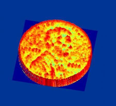
This 3D scan of a U.S. penny was created with a tiny camera chip developed at the California Institute of Technology (Caltech).
U.S. researchers have developed a camera chip that could give smartphones the ability to take 3D scans of everyday objects, a sought-after feature in the 3D-printing world.
Engineers at the California Institute of Technology (Caltech) said their device is based on a cheap silicon chip less than 1 millimeter square and it can produce 3D scans with extremely fine resolution.
The chips could be incorporated into phones and the data could be sent to 3D printers to duplicate scanned objects, eliminating the need to use large desktop devices.
The device works by shining beams of light, which are perfectly aligned, on a targeted object. It then detects subtle differences in the light that is reflected back from that object. The differences help it build a digital 3D image of the target.
To shine the light, the device uses an array of tiny LIDAR (light detection and ranging) laser beam scanners. Useful for measuring distance, LIDAR elements have been used for years in applications such as navigation for driverless cars and robots.
The light that is reflected off the object is picked up by a small 4 x 4 grid of detectors, as the researchers describe in a study published in the journal Optics Express..
The detectors act like pixels in that they measure the phase, frequency and intensity of the incoming light and assign a distance value to each pixel in the 3D image of the object that has been scanned.
The researchers used the proof of concept camera chip to create a 3D scan of a U.S. penny from half a meter away. The scan features micron-level resolution as well as the larger undulations on the penny's surface that are nearly invisible to the naked eye.
The 16-pixel array could be increased to hundreds of thousands to create larger, more powerful arrays for applications such as helping driverless cars avoid obstacles, according to Caltech.
"The small size and high quality of this new chip-based imager will result in significant cost reductions, which will enable thousands of new uses for such systems by incorporating them into personal devices such as smartphones," Caltech electrical engineering professor Ali Hajimiri said in a release last week.
Tim Hornyak covers Japan and emerging technologies for The IDG News Service. Follow Tim on Twitter at @robotopia.
Join the CIO Australia group on LinkedIn. The group is open to CIOs, IT Directors, COOs, CTOs and senior IT managers.